In the world of electronics, the demand for smaller and more powerful devices continues to grow. This has led to the development of High Density Interconnect (HDI) PCBs, which offer a solution to the increasing need for compact and high-performance circuit boards.
What is HDI PCB?
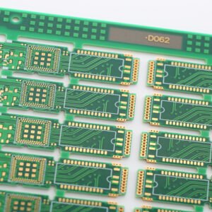
High Density Interconnect (HDI) PCB is a type of printed circuit board that allows for the miniaturization of electronic devices by increasing the density of components and connections. Unlike traditional PCBs, HDI PCBs use advanced manufacturing techniques to achieve a higher level of complexity in a smaller form factor.

HDI PCBs are designed to have multiple layers of circuitry, with microvias and fine-pitch components that enable the routing of signals and power in a more efficient manner. These boards are known for their high-density layout, which allows for more functionality in a limited space.
Advantages of HDI PCBs
There are several advantages to using HDI PCBs in electronic devices:
- Increased Component Density: HDI PCBs allow for the placement of more components in a smaller area, which results in smaller and more compact devices.
- Better Signal Integrity: The use of microvias and fine-pitch components in HDI PCBs reduces the length of signal paths, minimizing the risk of signal degradation and improving overall signal integrity.
- Improved Thermal Management: HDI PCBs enable the efficient dissipation of heat, thanks to their smaller size and increased surface area. This is especially important in devices with high power requirements.
- Enhanced Electrical Performance: The shorter interconnects and reduced parasitic capacitance and inductance in HDI PCBs result in improved electrical performance, such as faster signal transmission and reduced electromagnetic interference.
- Reliable and Durable: HDI PCBs are designed to withstand the demands of modern electronic devices, offering better resistance to environmental factors like temperature, humidity, and vibration.
Types of HDI PCBs
There are different types of HDI PCBs, each catering to specific design requirements:
- 1+N+1: This type of HDI PCB has a single build-up layer with stacked microvias, allowing for high-density routing between layers.
- 2+N+2: The 2+N+2 HDI PCB has two build-up layers, making it suitable for complex designs that require increased component density.
- 3+N+3: With three build-up layers, the 3+N+3 HDI PCB offers even higher component density and more routing options.
Applications of HDI PCBs
HDI PCBs find applications in various industries and electronic devices, including:
- Smartphones and tablets
- Laptops and computers
- Medical devices
- Automotive electronics
- Aerospace and defense systems
- Internet of Things (IoT) devices
The compact size, improved performance, and reliability of HDI PCBs make them ideal for these applications, where space constraints and high functionality are crucial.
In Conclusion
High Density Interconnect (HDI) PCBs have revolutionized the electronics industry by enabling the development of smaller, more powerful, and efficient devices. With their increased component density, improved signal integrity, and enhanced electrical performance, HDI PCBs are a vital component in the advancement of technology.
As the demand for smaller and more feature-rich devices continues to grow, HDI PCBs will play a significant role in meeting these requirements and driving innovation in the electronics industry.