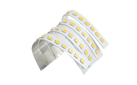
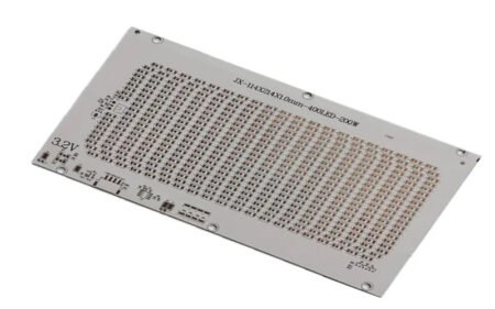
Metal PCB

HomeMetal PCB
ItemSpeci.
Layers1-6 layers
Board thickness0.6mm-7.0mm
MaterialAl Base, Cu Base, Fe Base, Ceramic Base Tg,Rogers
Max panel size600*1200mmm
Min hole size0.075mm
Min line width2mil
Surface finishHAL(with Pb free), Plated Ni/Au, ENIG, Immersion Tin,Immersion Ag OSP etc.
Copper thickness0.5-15 OZ
SoldermaskYellow, Red, White, Black, Blue, Green, Grey etc.
SilkscreenRed/Yellow/Black/White
Min PAD5mil(0.13mm)
Inter packageVacuum
Outer packageCarton
Outline tolerance±0.075mm
Hole tolerancePTH:±0.05 NPTH:±0.025
CertificateUL, IATF16949, ISO, RoHs&Reach
Special requestBlind hole+Gold finger + BGA
Material SuppilersShengyi, KB, Nanya, ITEQ,etc.

If you have any requirements for PCB/ PCBA/Components, please contact us and we will reply to you as soon as possible!

    Manufacturing of Metal PCB

    Making a metal printed circuit board (PCB) involves several steps similar to traditional PCB manufacturing, with some modifications to accommodate the metal core.

    • Copper Foil Lamination: Apply copper foil onto the dielectric layer using lamination techniques. The copper foil serves as the conductive layer where the circuit traces will be etched. Ensure proper adhesion between the copper foil and the dielectric layer.
    • Photoresist Application: Apply a layer of photoresist material onto the copper foil. This layer will be exposed to UV light through a photomask, defining the pattern of the circuit traces.
    • Exposure and Development: Expose the photoresist layer to UV light through a photomask that contains the desired circuit pattern. After exposure, the photoresist is developed to remove the unexposed areas, leaving behind the pattern of circuit traces.
    • Etching: Etch away the unwanted copper from the substrate using an etchant solution. The areas protected by the developed photoresist remain intact, defining the circuit traces on the PCB.
    • Final Processing: Remove the remaining photoresist and any etchant residues from the PCB. Inspect the board for any defects or irregularities.

    Yuanjin Technology are some key steps to ensure the production of a high-quality Metal PCB products:

    • Design: Begin by designing the PCB layout using specialized software. Considerations for thermal management and heat dissipation should be taken into account during the design phase, as metal PCBs are often used in applications where heat is a concern.
    • Material Selection: Choose the appropriate metal core material based on the specific requirements of your application. Aluminum is commonly used due to its lightweight and good thermal conductivity, but copper and alloys are also options.
    • Preparation of Metal Core: The metal core is typically prepped by cleaning and smoothening the surface. This may involve processes such as degreasing, brushing, and chemical treatment to ensure good adhesion of the dielectric and copper layers.
    • Dielectric Layer Application: Apply a thin layer of dielectric material onto the metal core. This dielectric layer serves as electrical insulation between the metal core and the copper traces. Common dielectric materials include epoxy-based resins or thermally conductive dielectrics for improved heat dissipation.

    What Do Our Customers Say?